
· 01 CATEGORY
Dielectric inks and varnishes for printed circuits
Dielectric inks and varnishes for printed electronics, designed to create electrical insulation layers in multilayer and flexible printed circuits. These formulations complement silver and carbon conductive inks in the manufacture of printed electronic devices.
Part of our range: Conductive inks for printed electronics
· 02
Typical applications
Use cases
- 01
Multilayer circuit insulation
Dielectric inks and varnishes can be considered to separate conductive layers in a printed architecture.
· 04
Ranges
Category products2 REF.
· 05
Related articles
- 01
- 02
Printed electrical insulation: the role of the dielectric layer
A dielectric ink is screen-printed between two conductive layers to provide printed electrical insulation: it prevents short circuits where tracks cross and allows several levels to be stacked in a multilayer circuit. The dielectric varnish is selected according to the associated conductive ink, the substrate and the constraints of the device: flexibility, thermal resistance, curing compatibility.
VFP formulations are developed to work with the silver and carbon conductive inks of the range, on flexible printed circuits as well as rigid substrates. Exact characteristics are given in the technical data sheet of each grade.
Selecting a dielectric grade
A dielectric layer is selected together with the associated conductive inks, substrate and the complete curing cycle. For a multilayer or flexible circuit, compatibility between layers, adhesion and processing conditions must be checked for the grade and final assembly.
See also the conductive range: Conductive inks for printed electronics.
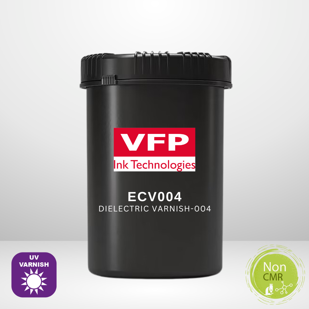
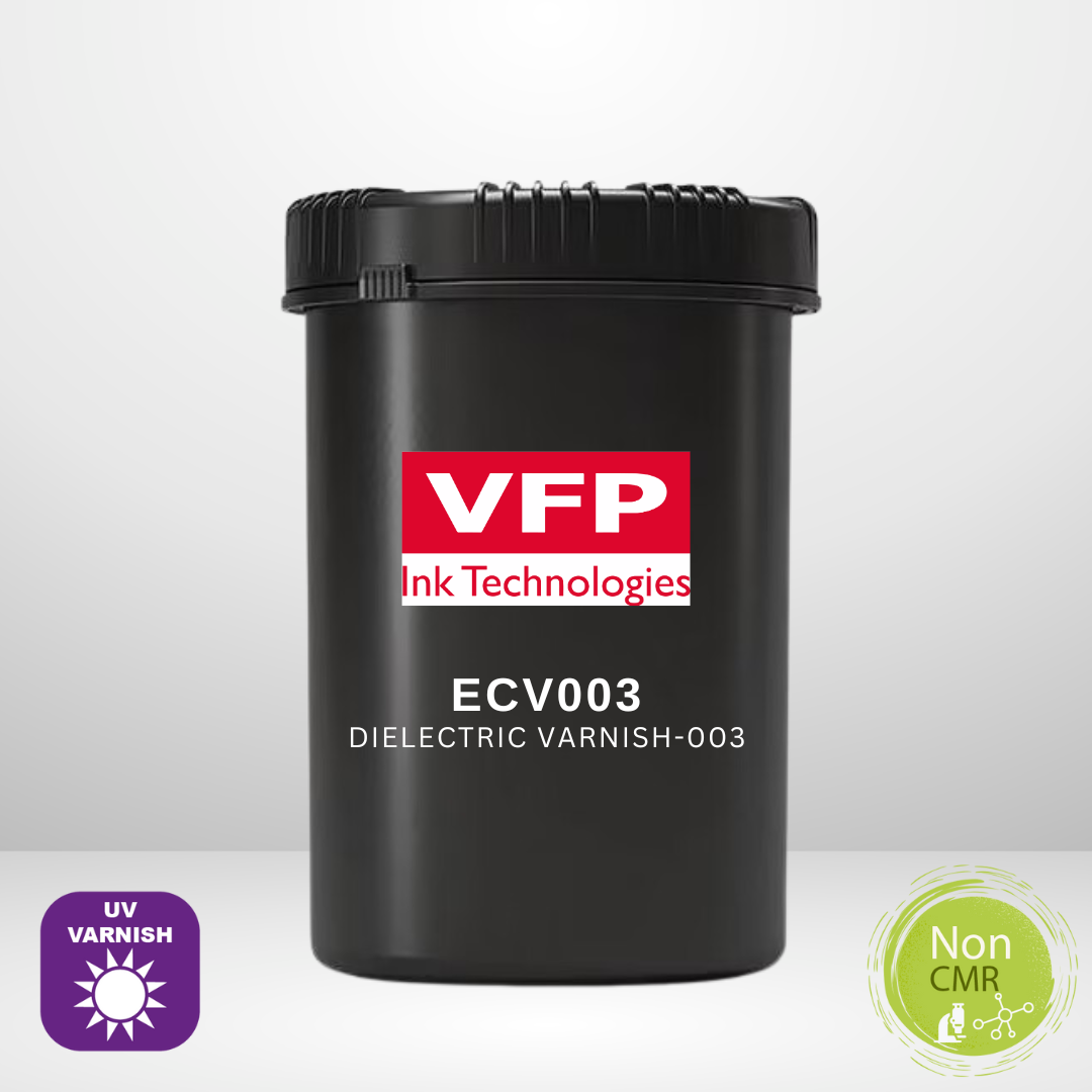
Grades and technical data sheets to consult: ECV003 (TDS), ECV004 (TDS).
Selection questions
- How can the appropriate grade be confirmed?
Compare the required function, substrate, process and curing conditions with the grade’s technical data sheet, then qualify the actual assembly.
Need a custom formulation?
Our technical sales team supports you from formulation selection through to industrial validation.